


PMPB11EN,115
N-Channel 30 V 9A (Ta) 1.7W (Ta), 12.5W (Tc) Surface Mount DFN2020MD-6
Availability: Out of Stock
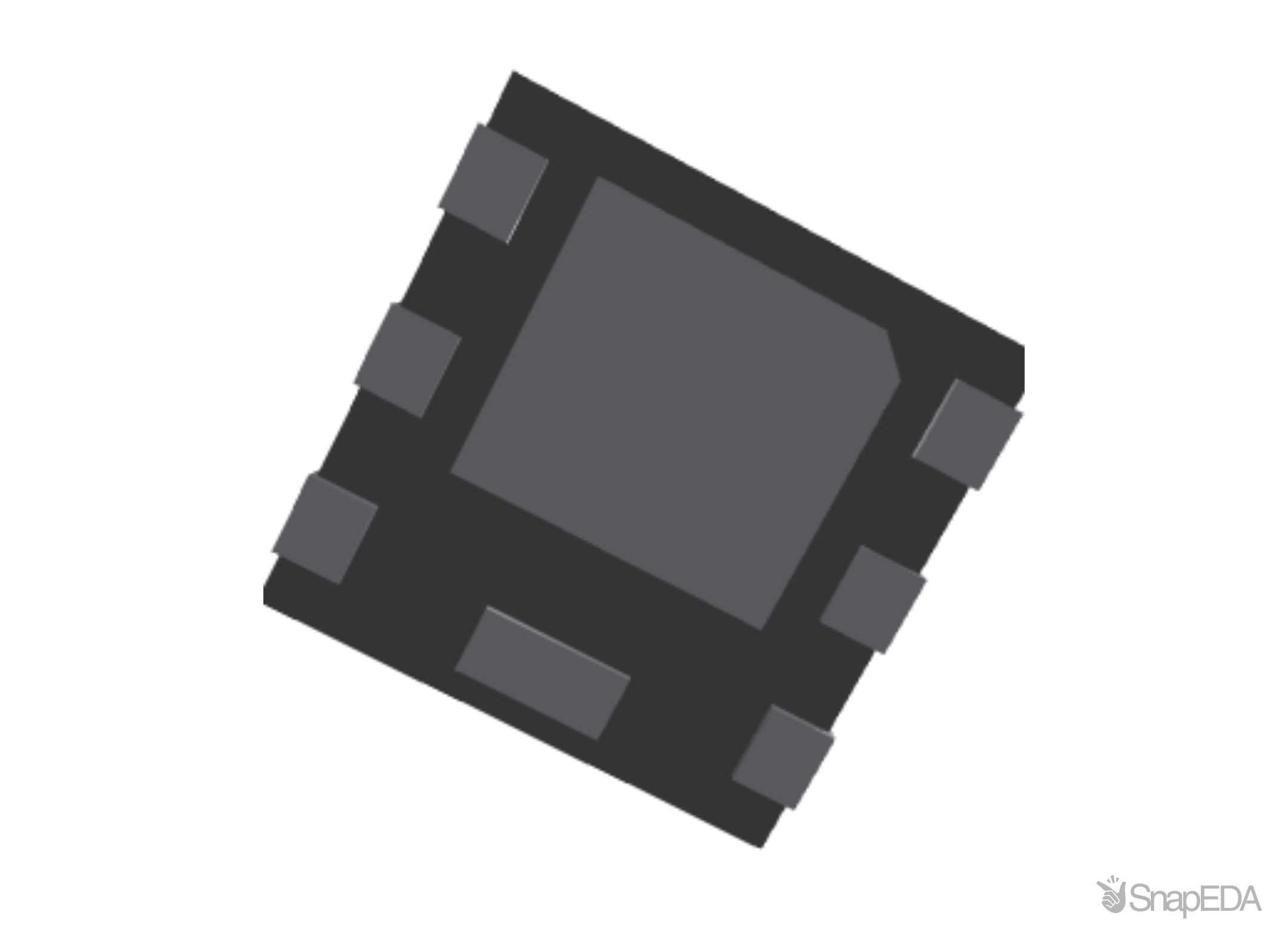
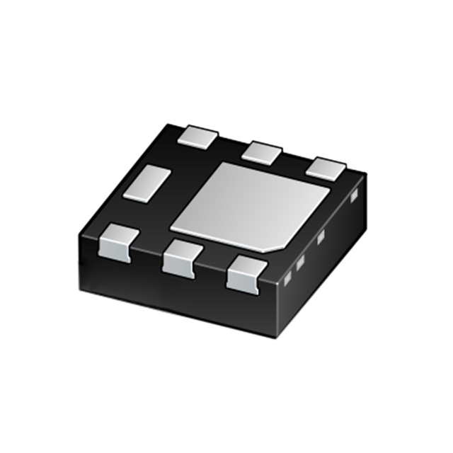
Package Type: DFN2020MD?6-6
CAD Models: Symbol, Footprint, 3D Model
What is SnapMagic Search?
SnapMagic Search is a free library of symbols & footprints for the PMPB11EN,115 by Nexperia and for millions of electronic components.
Compatible with Eagle, Altium, Cadence OrCad & Allegro, KiCad, & more.
Discover parts from Texas Instruments, Microchip, TE Connectivity, Vishay & more.
- Symbol and Footprint
- 3D Model
Symbol

No web preview
This Symbol is Available for
Footprint

No web preview
This Footprint is Available for
3D Model
Preview not available
Note: If you're using IE or Edge, right-click and choose "Save as" to download.
Get this 3D Model in 1 business day!

More


| Verification | Issues | Specs | Pricing |
Specifications for the PMPB11EN,115
| Part Name | PMPB11EN,115 |
| Manufacturer | Nexperia USA |
| Formats Available for Symbols and Footprints |
Altium, Eagle, KiCAD, Cadence OrCad/Allegro, PADS, DxDesigner, PCB123, Pulsonix, Proteus |
| Maximum Drain Source Voltage (V) | 30 V |
| Maximum Continuous Drain Current (A) | 9 A |
| Mounting Type | Surface Mount |
| Maximum Gate Source Voltage (V) | -20 V, +20 V |
| Maximum Power Dissipation | 12.5 W |
| Transistor Material | Si |
| Maximum Gate Threshold Voltage (V) | 2 (V) |
| Channel Mode | Enhancement |
| Height | 0.65 (mm) |
| Width | 2.1 (mm) |
| Length | 2.1 (mm) |
| Maximum Drain Source Resistance | 14.5 mΩ |
| Package Type | DFN2020 |
| Number Of Elements Per Chip | 1 |
| Minimum Operating Temperature | -55 °C |
| Minimum Gate Threshold Voltage (V) | 1 (V) |
| Typical Gate Charge Vgs | 13.7 nC @ 10 V |
| Channel Type | N |
| Maximum Operating Temperature | +150 °C |
| Pin Count | 8 |
| Transistor Configuration | Single |


No issues have been reported for the PMPB11EN,115
If you experienced any issues with the symbol or footprint, please report it.